Features
Business
Research
Technology talk
Highlights from the NAPIM Fall Technical and the Ink World Printed Electronic/eInk Conferences
February 13, 2020 By Martin Habekost
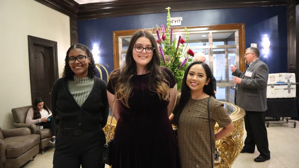 Ryerson GCM students (left to right) Layla Abdi, Catherine Di Luca and Pauline Reyes at the NAPIM conference. Photos: Martin Habekost
 From October 15 to 18, 2019, three students from Ryerson University’s School of Graphic Communications Management (GCM) and I attended the National Association of Printing Ink Manufacturers’ Fall Technical Conference for the first time. NAPIM was founded in 1916 and its mission is to “promote the general development and improvement of member companies by fostering greater understanding and knowledge of the printing ink industry as well as representing the industry as a whole on a national basis.”
It’s an interesting story how this connection came together. During the TAGA Annual Technical Conference, Juanita Parris from Sun Chemical, who is also the President of the National Printing Ink Research Institute (NPIRI), asked if I could give her one of my business cards because NAPIM and NPIRI would like to get more involved with universities and students. Later, I was contacted by George Fuchs from NAPIM and arrangements were made so that Ryerson GCM students and I could attend the conference. The NAPIM conference was held outside of Chicago in Oak Brook, Ill.
The keynote presentation for the NAPIM conference was on how paper stimulates all our senses when we read. Delivered by David Sullivan from Sappi Paper, the presentation noted that we have increased information retention when we read something that is printed. Not only do we retain information better, it also has a calming influence on us. When we read something on a screen, we switch to a skimming mode, where we just try to look for the important parts. Sullivan’s main point was that reading information on paper helps us comprehend and retain information better.
The next presentation was about sustainability from a printer’s perspective. Laura Rowell from Sonoco predicted that by 2025, we will have 100-percent reusable, recyclable or compostable plastic packaging. Many major brands are already on board and are working towards this goal. She also stated that printing inks should not contaminate the recycling process.
Lee Marcoe from Lake County Press gave a very informative talk about “hot topics” their clients are asking for. Until 2009, their clients were demanding sustainable substrates and insisted that the energy used to print their jobs came from wind energy. Prior to 2010, customers demanded soy-based inks, vegetable inks, low VOC or VOC-free inks. All these requests are not top of mind anymore, but there has been an uptake in litho printing and direct mailings, Marcoe said. Direct mailings are now more targeted than before, resulting in more customized campaigns.
After these presentations, it was my turn to introduce Ryerson University and the Graphic Communications Management program to the audience. Not many attendees were familiar with us. The audience was also introduced to the two Material Science courses that are part of the curriculum. At the end of my presentation, I shared the project that students Layla Abdi, Catherine Di Luca and Pauline Reyes – who attended the conference – did in their Advanced Material Science course. The students prepared posters about their projects that were displayed during the tabletop presentations at the end of the first day.
John Jilek from Ink Solutions and Bill Giczkowski from INX International gave a presentation on the state of the industry. They noted that overall, the ink industry has an optimistic outlook for the future. Their main concerns are raw material costs and the availability of raw materials. As well, healthcare costs and transportation costs are also issues on their radar. Ink companies are committed to consistent product quality, competitive prices and tech support. The number of ink companies went down from 397 in 2014 to 192 in 2016. Also the number of print companies is down, but there is a slight upwards trend in ink sales.
The next day’s presentations were more on the technical side. Darren Gapen from WestRock introduced the company to the attendees. Did you know that WestRock has more than 320 manufacturing sites worldwide? Gapen demonstrated the many raw materials the company uses everyday and the other products, mainly solid bleached sulfate (SBS), that it manufactures. The numbers are mind-boggling. One surprising fact is that WestRock produces 18,000 t of air filter paper for furnaces every year.
Up next was a presentation by Sanjay Monie from Orion Engineered Carbons, formerly known as Degussa. His presentation gave an overview on how different types of carbon black are made and what their applications are. Carbon black can be surface-treated to make the material more polar, so it is easier to incorporate into different materials. Carbon black is also used for non-impact printing applications and Orion also manufactures a food packaging-compliant carbon black. It was interesting to learn how certain types of carbon black are surface-treated so they can be incorporated into waterborne inkjet inks.
Rachel Schwen from the Sherwin-Williams Performance Coatings Group spoke about colour measurement in the industry. First she spoke about colour, how humans perceive colour, how colour is measured, and how modern light sources, like LEDs, influence the way colour is seen and measured, since LED illuminants find their way into measurement devices. Her presentation also highlighted small and relatively inexpensive colour measurement devices, such as ColorMuse, Nix and Capsure. She said these devices are great to get a general idea about a colour, but are not a replacement for colour measurement devices from manufacturers like X-Rite, Techkon or Konica Minolta.
Jennifer Heathcote from Eminence UV gave a very detailed presentation about UV-LED curing. UV-LEDs were not able to produce UV-C light until recently, but these LEDs are not as powerful yet, as they need to be. She predicted that 275 nm UV-C LED curing will coming to the market in the near future. UV-LEDs are usually placed 15 mm above the web surface and sometimes at a distance of 25 mm to 100 mm. This is a lot closer than conventional mercury vapour lamps. If UV-LED is used for curing UV ink on 3D printed parts, the distance to the surface is usually 50 mm to 100 mm. An upcoming trend is also the inline measurement of UV intensity of the curing systems. Different systems are available that allow the inline control of the UV light intensity and energy density.
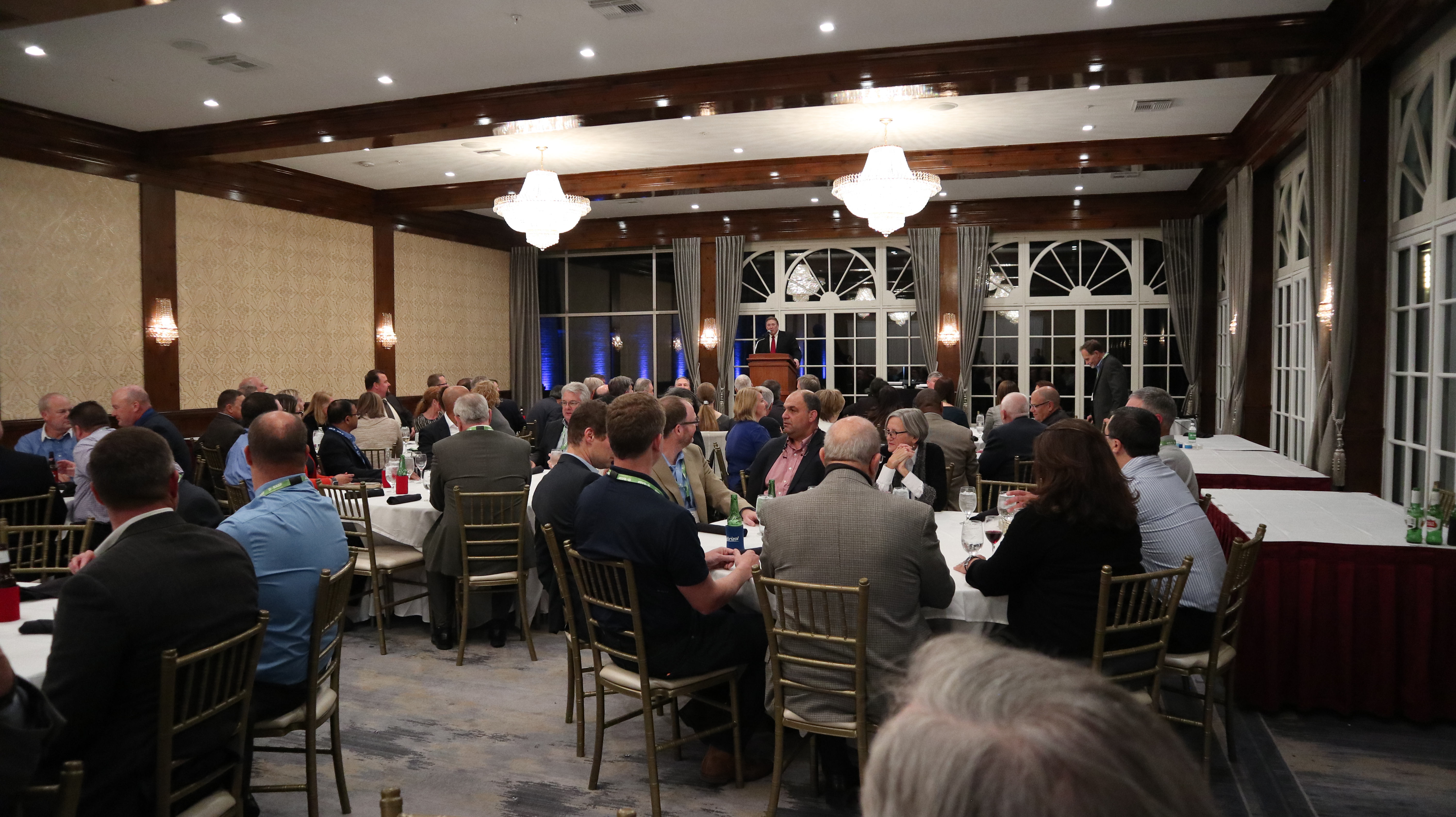
The remainder of the second day of the conference covered supply chain issues, smart manufacturing (also known as Industry 4.0) and inks for food contact. Inks for food contact are a very complex matter and as such, this presentation was given by a lawyer from a law firm that specializes in this area. The NAPIM conference concluded with a reception and an awards dinner.
John Copeland, NAPIM Executive Director (above), and Jim Leitch, NAPIM President and President of Braden Sutphin Ink (below), take the podium at the NAPIM awards dinner.

The following day and a half were dedicated to the Ink World Printed Electronic/eInk Conference. The keynote was given by Erika Rebrosova from Sun Chemical. She gave a very detailed and informative overview of printed electronics and eInks. There is a trend to use flexible circuit boards with screen printed silver-based inks. There is also the possibility of using materials called silver flex and copper flex to print electronic circuits. At the moment, it is not possible to make high power, high frequency, high density electronic circuits with silver-based inks. As I mentioned before, screen printing is the print process of choice for printed electronics, although some are done with inkjet or flexo technology. Conductive inks are made of conductive particles, resins and solvents. The conductive particles are silver, silver chloride, carbon black/graphite, conductive polymers, copper, silver-coated copper, graphene, carbon nano tubes and nickel. What is not possible at the moment is a UV-curable silver conductive ink. This is considered the Holy Grail of the printed electronics ink market.
Then, Robert Waldrop of DuPont Advanced Materials walked us through DuPont’s printed electronics history. It started in 1961 with screen-printed resistors and moved onto photovoltaic metallization in 1984, printed blood glucose sensors in 1985, printed electroluminescence in 1998 and printed heating elements in 1998. DuPont has also developed polyimide inks that can withstand temperatures of up to 320ºC, but cure at a low temperature of 60ºC to 100ºC. DuPont also has solutions for smart clothing. The challenge for smart clothing with electronic circuits is that the circuits need to be able to withstand stretching and washer and dryer cycles without breaking, which would render them unusable.
Casey Grenier from Tekscan presented the printed force sensor technology. The force sensors are also screen-printed. They are force-sensitive resistors that can be used in robotic surgical systems, wearable pump manufacturers, an impact-sensitive organ transplant container or force-sensitive theft detection.
Chris Booher from ChemCubed talked about jettable solutions for printed electronics. He spoke about 3D jettable solutions for rigid and flexible substrates using nano-particle free silver conductive ink. The ink needs to get sintered at 80ºC, meaning that only after the sintering process will the printed circuit function. The company also has a so-called NanoJet aerosol spray printing technology which allows them to print resistors and capacitors with low production variances, almost like conventional manufacturing of these electronic components. They are currently working on flexible, extensible inks that allow for a stretch of 130 percent.
I mentioned the sintering process before. It’s an important step to have printed electronic circuits conduct electricity. The sintering can be done either through temperature, basically “baking” the conductive particles together or through photonic sintering. This process delivers a very intense light pulse onto the printed circuit, fusing the particles together. Lou Panico from Xenon Corporation presented the technology his company can manufacture for the photonic sintering process. Panico gave the comparison of delivering 100 Joules of light energy. You can do this by shining a 10W light for 10 seconds or 1 megawatt for 1 µs. The latter is used in photonic sintering. Photonic sintering reduces the curing (sintering) time from up to 30 minutes to less than 10 seconds, an important timegain for the mass production of printed electronics.
A few presentations focused on wearable printed electronics. There are a few takeaways from these sessions. Fashion and electronics engineers are starting to collaborate on designing wearable printed electronics. Wearable electronics will be part of the Internet of Things (IoT). They can also be used to monitor the health of the person wearing the clothing with circuits and sensors in the fabric. Besides manufacturing fabrics and printing circuits on them, thin lightweight and renewable power sources also need to be made. As of now, wearables do not have the consumer market pull yet.
Overall both conferences were very interesting and opened my mind to new topics that relate to printing. It was worth attending these conferences and I thank NAPIM and Ink World Magazine for making it possible for the students and I to attend.
This article was originally published in the January/February 2020 issue of PrintAction, now available online.
Print this page